Below are the questions asked during the event, along with their respective answers.
Q: We are designing a power Mosfet switching IC with 5 V output voltage and 1.2 amps o/p current. How to calculate power dissipation for this chip and how to select a correct package with proper thermal resistance value to dissipate the heat.
A: The switching frequency can influence the effective thermal resistance for the device. Designing for the “always on” scenario can lead to significant over-design so it is important to include the switching effect. It is difficult to provide much of an answer without knowing more details but it seems to indicate that some sort of thermal analysis is required to develop a proper thermal design.
Q: Can you just capture thermal vias under the device using thermal territory in FloTHERM XT? This will be useful during early design phase when component placement is available but not detailed traces.
A: There are methods of including the effective thermal conductivities in localized areas using SmartParts available in FloTHERM and FloTHERM XT. Also, the vias can be modeled discretely as defined by the thermal engineer. Currently Thermal Territories don’t differentiate between vias and traces.
Q: Shouldn’t the junction temperature drop when inflation distance through board is increased (increased copper content)? Slide shows it otherwise.
A: It depends on the density of copper beneath the component as compared to the rest of the PCB on that layer. If there is a lot of copper beneath the component then resolving it explicitly will lower the component temperature. If there isn’t much copper then the junction temperature will increase.
Q: Are territories already available in V12?
A: Thermal Territories, as discussed in the seminar, is a technology that is provided in FloTHERM XT. FloTHERM has a different methodology for capturing detailed trace information and is described below.
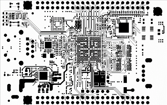
Q: Can you do Explicit Traces in FloTHERM?
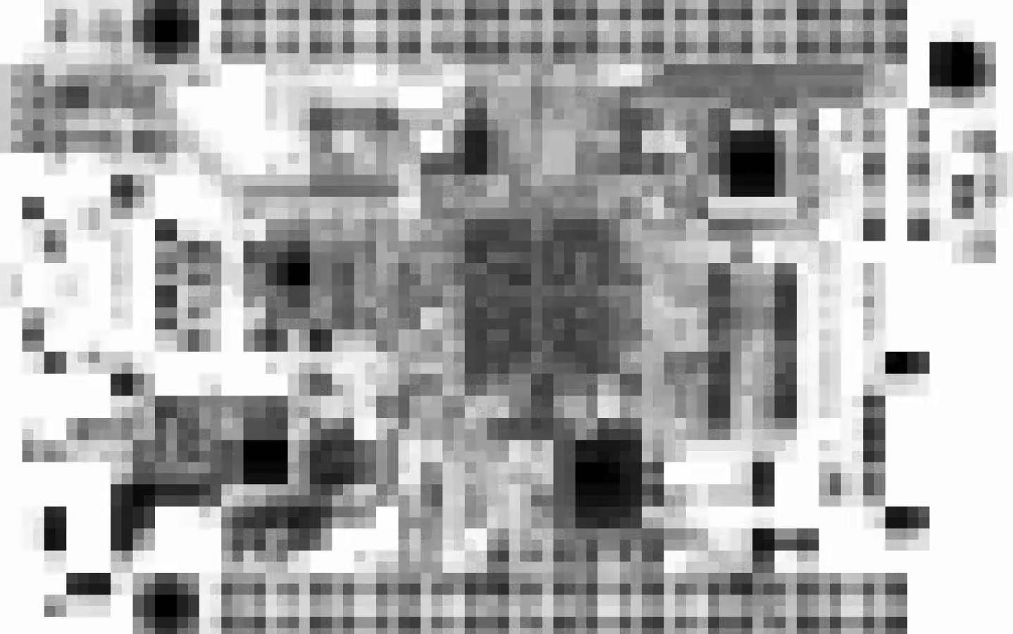
A: Explicit traces can be modeled in FloTHERM using a script that is provided with FloTHERM. The workflow provided within FloTHERM, by way of the FloEDA Bridge, is to resolve the traces as a number of patches, or regions of effective thermal conductivities, as shown in the images below. The user can control the number of patches to resolve the areas of varying conductor density.
Q: Are there any comparisons with testing data?
A: I am not aware of any specific comparisons. I have modeled traces explicitly when correlating against measurement for IC thermal characterizations. Explicit copper will provide the most accuracy and any assumption on the effective thermal conductivity used in a thermal model will introduce some level of error. The amount of error is very case dependent.
Q: What makes adding more details on layer 6 have higher Tj? Can it be generalized? Does it mean that we need to put some guard-band on results with simplified effective K?
A: In my Thermal Territory example I resolved to layer 4, and another example resolved to layer 6. I neglected to provide an example of resolving to layer 5. What I believe we are noticing is that when resolving to layer 4, layer 5 had the artificial benefit of the effective thermal conductivity associated with that layer. When resolving to layer 6, layer 5 is also resolved explicitly but there wasn’t a significant amount of Copper on layer 5 so the net effect is a reduced thermal conductivity. I think it is difficult to generalize other than to say that explicitly modeling copper will provide the most accuracy and effective thermal conductivities will always introduce some error. A lot of thermal design occurs well before any PCB has been routed so both approaches are useful but at different parts of the design process.
Q: How do you account for the effect of thermal vias for effective thermal conductivity calculations?
A: Typically by assuming a percent coverage of vias for the particular dielectric layer. The thru-plane effective thermal conductivity would be calculated as conduction in parallel with the dielectric. In-plane conductivity would be calculated as conduction in series with the dielectric. Assuming a PCB is using FR4 and Copper, and a 1% coverage of vias, the thru-plane thermal conductivity would be about 3 W/mK and the in-plane would be about 0.3 W/mK.
Q: Assuming 10% copper for a board seems a bit low is there a range you would recommend?
A: If the PCB is modeled as a single block of effective thermal conductivity an assumption of 10-20 % conductor by volume is reasonable. There is a significant improvement in accuracy if the PCB is modeled as detailed, where each layer is modelled individually with an effective thermal conductivity. When modeling the layers individually a power or ground layer typically is 70-100 % conductor by volume and signal layers from 10-30 % conductor by volume. These are meant as reasonable assumptions to be used before more detailed information becomes available.
Q: What would be a typical mesh size (# elements) for the example you showed using the various techniques?
A: Generally speaking when modeling PCBs with effective thermal conductivities the mesh size is on the order of 1,000s, image processing on the order of 10,000s, and explicit traces on the order of 100,000s.